Recent advances in gun brightness have enabled aberration corrected scanning TEMs to pack 1 nA of current into a 1 Ångstrom probe. We now need detectors that can take advantage of these high beam currents to provide rapid and complete phase-space information from scattering experiments for imaging the structure and properties of materials at the atomic scale.
Cornell’s Detector Group
The Detector Group laboratory, led by Physics Professors Julia Thom-Levy and Sol Gruner, supports a resident staff of highly experienced detector professionals, including Drs. Mark Tate, Hugh Philipp and Kate Shanks and Mr Martin Novak. It is housed in Clark Hall which has fully equipped professional and student shops, stockrooms, and chemical and electronics facilities. We have worked with the detector group for over 15 years to develop direct electron detectors for electron microscopy, including the Electron Microscope Pixel Array Detector (EMPAD) and the EMPAD-G2.
Pixel Array Detectors for Electron Microscopy
EMPAD technology has been successfully demonstrated for 4D-STEM, mainly due to its high dynamic range, high speed and large pixel size. This has been a key enabling technology for many of our electron microscopy “firsts”, including the Guinness world record for spatial resolution. The Cornell EMPAD was licensed to TFS/FEI, with first sales in late 2017. The EMPAD received a 2019 Microscopy Today Innovation Award.
Spectroscopy
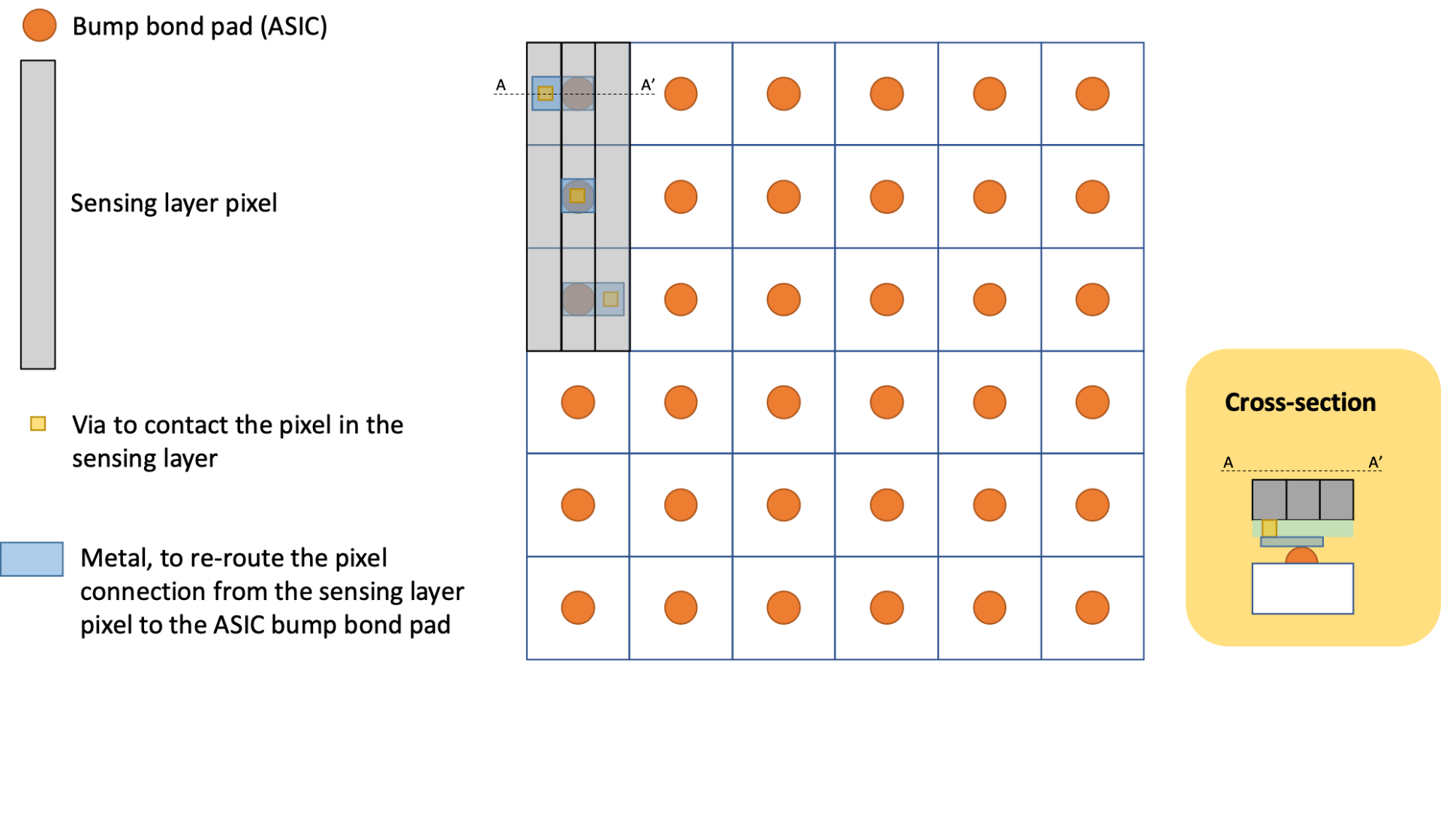
The EMPAD design can also be remapped for electron energy loss spectroscopy (EELS). The high saturation current and high dynamic range makes the EMPAD technology well suited to the large intensity range spanned by a typical EELS spectrum, with high intensity in the zero loss peak (ZLP), and single electron counts at core edges. The goal is to collect ZLP and all inelastically scattered electrons out to a few kilovolts. Consequently, for EELS applications it is advantageous to have a large pixel array thus increasing the energy field of view. In order to keep the total chip dimensions within the standard size of the microscope and still make use of the EMPAD ASIC technology, we propose a re-pixelation of the top sensing layer of the bump-bonded assembly: smaller pixels can be defined in the top layer and re-mapped onto the regular ASIC pixels. The re-pixelation can be such that all pixels have the same dimension, with no gaps. Further, more ASICs can be tiled up together to create a larger array. This is an exploratory collaboration with TFS.