Xiong, Y., Y. Yang, H. Joress, E. Padgett, U. Gupta, V. Yarlagadda, D. N. Agyeman-Budu, X. Huang, T. E. Moylan, R. Zeng, A. Kongkanand, F. A. Escobedo, J. D. Brock, F. J. DiSalvo, D. A. Muller, and H. D. Abruña. “Revealing the Atomic Ordering of Binary Intermetallics Using in Situ Heating Techniques at Multilength Scales” Proceedings of the National Academy of Sciences 116, (2019), 1974–1983. Available at http://www.pnas.org/lookup/doi/10.1073/pnas.1815643116
A. K. Yadav, K. X. Nguyen, Z. Hong, P. García-Fernández, P. Aguado-Puente, C. T. Nelson, S. Das, B. Prasad, D. Kwon, S. Cheema, A. I. Khan, C. Hu, J. Íñiguez, J. Junquera, L.-Q. Chen, D. A. Muller, R. Ramesh, and S. Salahuddin. “Spatially Resolved Steady-State Negative Capacitance” Nature (2019): 1. Available at http://www.nature.com/articles/s41586-018-0855-y
Schaab, J., S. H. Skjærvø, S. Krohns, X. Dai, M. E. Holtz, A. Cano, M. Lilienblum, Z. Yan, E. Bourret, D. A. Muller, M. Fiebig, S. M. Selbach, and D. Meier. “Electrical Half-Wave Rectification at Ferroelectric Domain Walls” Nature Nanotechnology (2018), https://doi.org/10.1038/s41565-018-0253-5
S. Im, Z. Chen, J. M. Johnson, P. Zhao, G. H. Yoo, E. S. Park, Y. Wang, D. A. Muller, and J. Hwang. “Direct Determination of Structural Heterogeneity in Metallic Glasses Using Four-Dimensional Scanning Transmission Electron Microscopy” Ultramicroscopy 195, (2018), 189–193.

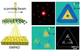
Y. Jiang, Z. Chen, Y. Han, P. Deb, H. Gao, S. Xie, P. Purohit, M. W. Tate, J. Park, S. M. Gruner, V. Elser, and D. A. Muller. “Electron Ptychography of 2D Materials to Deep Sub-Ångström Resolution” Nature 559, no. 7714 (2018): 343–349. doi:10.1038/s41586-018-0298-5.
Y. Han, K. Nguyen, M. Cao, P. Cueva, S. Xie, M. W. Tate, P. Purohit, S. M. Gruner, J. Park, and D. A. Muller, “Strain Mapping of Two-Dimensional Heterostructures with Subpicometer Precision”. Nano Letters (2018). DOI:10.1021/acs.nanolett.8b00952
J. Xiao, H. Zhu, Y. Wang, W. Feng, Y. Hu, A. Dasgupta, Y. Han, Y. Wang, D. A. Muller, L. W. Martin, P. Hu, and X. Zhang, “Intrinsic Two-Dimensional Ferroelectricity with Dipole Locking”. Physical Review Letters 120, 227601 (2018). DOI:10.1103/PhysRevLett.120.227601
X.-C. Liu, Y. Yang, J. Wu, M. Liu, S. P. Zhou, B. D. A. Levin, X.-D. Zhou, H. Cong, D. A. Muller, P. M. Ajayan, H. D. Abruña, and F.-S. Ke, “Dynamic Hosts for High-Performance Li–S Batteries Studied by Cryogenic Transmission Electron Microscopy and in Situ X-ray Diffraction”. ACS Energy Letters, 1325-1330 (2018).
S. Xie, L. Tu*, Y. Han*, L. Huang, K. Kang, K. U. Lao, P. Poddar, D. A. Muller, R. A. DiStasio Jr., J. Park “Coherent Atomically-thin Transition-metal Dichalcogenide Supperlattices with Engineered Strain” Science 395, 1131-1136 (2018)
R. Yan, G. Khalsa, S. Vishwanath, Y. Han, J. Wright, S. Katzer, N. Nepal, B. P. Downey, D. A. Muller, H. G. Xing, D. J. Meyer, D. Jena “GaN/NbN Epitaxial Semiconductor/Superconductor Heterostructures” Nature 555, 183-189 (2018)
C. Zhang, M. Li, Y. Han, Y. Su, L. Li, D. A. Muller, J. Tersoff, C. Shih, “Strain distributions and their influences on electronic structures of WSe2-MoS2 laterally strained heterojunctions” Nature Nanotechnology 13, 152-158 (2018)
E. Padgett, N. Andrejevic, Z. Liu, A. Kongkanand, W. Gu, K. Moriyama, Y. Jiang, S. Kumaraguru, T.E. Moylan, R. Kukreja, D.A. Muller, “Connecting Fuel Cell Catalyst Nanostructure and Accessibility Using Quantitative Cryo-STEM Tomography”, Journal of the Electrochemical Society, doi: 10.1149/2.0541803jes (2018).
R. Rizo, R. Arán-Ais, E. Padgett, D. Muller, M.J. Lázaro, J. Solla-Gullon, J.M. Feliu, E. Pastor, H.D. Abruña, “Pt-richcore/Sn-richsubsurface/Ptskin nanocubes as highly active and stable electrocatalysts for the ethanol oxidation reaction”, Journal of the American Chemical Society, doi: 10.1021/jacs.8b00588 (2018).
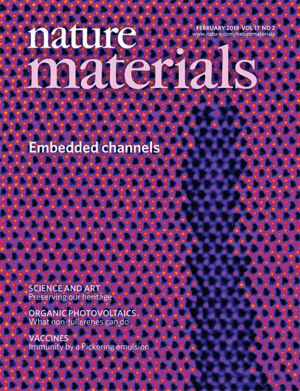
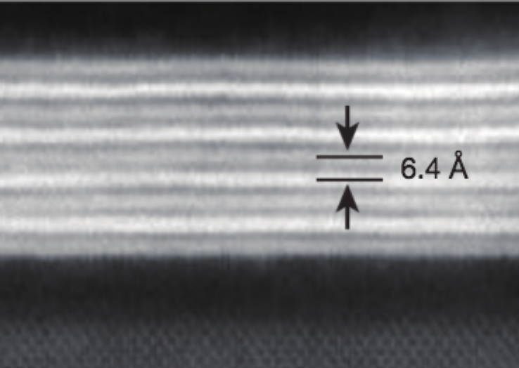
Y. Han, M.-Y. Li, G.-S. Jung, M. A. Marsalis, Z. Qin, M.J. Buehler, L.-J. Li, D.A. Muller, “Sub-nanometer channels embedded in two-dimensional materials” Nature Materials 17, 129-133 (2018).

M. Z. Miskin, K. J. Dorsey, B. Bircan, Y. Han, D. A. Muller, P. L. McEuen, and I. Cohen, “Graphene-based bimorphs for micron-sized, autonomous origami machines”. Proceedings of the National Academy of Sciences 115, 466-470 (2018). DOI:10.1073/pnas.1712889115

B.D.A. Levin, Y. Jiang, E.Padgett, S. Waldon, C. Quammen, C. Harris, U. Ayachit, M. Hanwell, P. Ercius, D.A. Muller, R. Hovden, “Tutorial on the Visualization of Volumetric Data Using tomviz“, Microscopy Today, doi: 10.1017/S1551929517001213 (2018)
A.M. Pasqualeti, E. Padgett, D.Y. Kuo, D.A. Muller, F.H.B. Lima, J. Suntivich, “Influence of Aliovalent Substitutions on Oxygen Reduction on Tantalum Oxynitrides”, Journal of the Electrochemical Society doi: 10.1149/2.1361706jes (2017)
V. Beermann, M. Gocyla, S. Kühl, E. Padgett, H. Schmies, M. Goerlin, N. Erini, M. Shviro, M. Heggen, R.E. Dunin-Borkowski, D.A. Muller, P. Strasser, “Tuning the Electrocatalytic Oxygen Reduction Reaction Activity and Stability of Shape-Controlled Pt–Ni Nanoparticles by Thermal Annealing − Elucidating the Surface Atomic Structural and Compositional Changes”, Journal of the American Chemical Society, DOI: 10.1021/jacs.7b06846 (2017).
Y. Jiang, E. Padgett, R. Hovden, D.A. Muller, “Sampling limits for electron tomography with sparsity-exploiting reconstructions” Ultramicroscopy, https://doi.org/10.1016/j.ultramic.2017.12.010 (2017)

E. Padgett, R. Hovden, J.C. DaSilva, B.D.A. Levin, J.L. Grazul, T. Hanrath, D.A. Muller, “A Simple Preparation Method for Full-Range Electron Tomography of Nanoparticles and Fine Powders” Microscopy and Microanalysis, doi:10.1017/S1431927617012764 (2017)
W. Jin, S. Vishwanath, J. Liu, L. Kong, R. Lou, Z. Dai, J. T. Sadowski, X. Liu, H. Lien, A. Chaney, Y. Han, M. Cao, J. Ma, T. Qian, J. I. Dadap, S. Wang, M. Dobrowolska, J. Furdyna, D. A. Muller, K. Pohl, H. Ding, H. G. Xing, R. M. Osgood, Phys. Rev. X, 7, 041020 (2017)
Y. Ji, B. Calderon, Y. Han, P. Cueva, N. R. Jungwirth, H. A. Alsalman, J. Hwang, G.D. Fuchs, D.A. Muller, M.G. Spencer. ACS Nano 11, 12057-12066 (2017)
Y. Tsai, Z. Chu, Y. Han, C.‐P. Chuu, D. Wu, A. Johnson, F. Cheng, M.‐Y. Chou, D. A. Muller, X. Li, K. Lai, C.‐K. Shih, “Tailoring semiconductor lateral multijunctions for giant photoconductivity enhancement” Advanced Materials 29, 1703680 (2017)
K. Kang, K.-H. Lee, Y. Han, H. Gao, S. Xie, D. A. Muller, J. Park, “Layer-by-layer assembly of two-dimensional materials into wafer-scale heterostructures” Nature 550, 229-233 (2017)
A. Lu, H. Zhu, J. Xiao, C. Chuu, Y. Han, M. Chiu, C. Cheng, C. Yang, K. Wei, Y. Yang, Y. Wang, D. Sokaras, D. Nordlund, P. Yang, D. A. Muller, M. Chou, X. Zhang, L. Li ” Janus Monolayers of Transition Metal Dichalcogenides” Nature Nanotechnology 12, 744-749 (2017)
J.A. Mundy, J. Schaab, Y. Kumagai, A. Cano, M. Stengel, I.P. Krug, D.M. Gottlob, H. Doğanay, M.E. Holtz, R. Held, Z. Yan, E. Bourret, C.M. Schneider, D.G. Schlom, D.A. Muller, R. Ramesh, N.A. Spaldin, D. Meier “Functional electronic inversion layers at ferroelectric domain walls” Nature Materials, doi:10.1038/nmat4878 (2017).
T. Sun, B.D.A. Levin, J. J. L. Guzman, A. Enders, D.A. Muller, L.T. Angenent & J. Lehmann, “Rapid electron transfer by the carbon matrix in natural pyrogenic carbon”, Nature Communications, 8, 14873 (2017).
B.D.A. Levin, M.J. Zachman, J.G. Werner, R. Sahore, K.X. Nguyen, Y. Han, B. Xie, L. Ma, L.A. Archer, E.P. Giannelis, U. Wiesner, L.F. Kourkoutis & D.A. Muller, “Characterization of Sulfur and Nanostructured Sulfur Battery Cathodes in Electron Microscopy Without Sublimation Artifacts” Microscopy and Microanalysis, 23, 155-162 (2017).
R. Sahore, B.D.A. Levin, M. Pan, D.A. Muller, F.J. DiSalvo, E.P. Giannelis, “Design Principles for Optimum Performance of Porous Carbons in Lithium–Sulfur Batteries”, Advanced Energy Materials, 6 (14), 1600134, (2016).
K. X. Nguyen, M. E. Holtz, J. Richmond-Decker, D. A. Muller, “Spatial Resolution in Scanning Electron Microscopy and Scanning Transmission Electron Microscopy Without a Specimen Vacuum Chamber”, Microscopy and Microanalysis, 22, 754-767 (2016).
B.D.A. Levin, E. Padgett, C-C. Chen, M.C. Scott, R. Xu, W. Theis, Y. Jiang, Y. Yang, C. Ophus, H. Zhang, D-H. Ha, D. Wang, Y. Yu, H.D. Abruña, R.D. Robinson, P. Ercius, L.F. Kourkoutis, J. Miao, D.A. Muller, R. Hovden, “Nanomaterial datasets to advance tomography in scanning transmission electron microscopy”, Sci Data, 3, 160041 (2016).
Y. Han, K. X. Nguyen, Y. Ogawa, J. Park, D. A. Muller, “Atomically Thin Graphene Windows That Enable High Contrast Electron Microscopy without a Specimen Vacuum Chamber”. Nano Letters, 16 (12), 7427, (2016).
C. Sun, D. L. Wakefield, Y. Han, D. A. Muller, D. A. Holowka, B. A. Baird, W. R. Dichtel, “Graphene Oxide Nanosheets Stimulate Ruffling and Shedding of Mammalian Cell Plasma Membranes”. Chem 1 (2), 273-286 (2016).
M. Zhao, Y. Ye, Y. Han, Y. Xia, H. Zhu, S. Wang, Y. Wang, D. A. Muller, X. Zhang, “Large-scale chemical assembly of atomically thin transistors and circuits”. Nature Nanotechnology 11, 954-959 (2016).
M. H. D. Guimarães, H. Gao, Y. Han, K. Kang, S. Xie, C. J. Kim, D. A. Muller, D. C. Ralph, J. Park, “Atomically-Thin Ohmic Edge Contacts Between Two-Dimensional Material”. ACS Nano 10 (6), 6392-6399 (2016).
J. A. Mundy, C. M. Brooks, M. E. Holtz, J. A. Moyer, H. Das, A. F. Rébola, J. T. Heron, J. D. Clarkson, S. M. Disseler, Z. Liu, A. Farhan, R. Held, R. Hovden, E. Padgett, Q. Mao, H. Paik, R. Misra, L. F. Kourkoutis, E. Arenholz, A. Scholl, J. A. Borchers, W. D. Ratcliff, R. Ramesh, C. J. Fennie, P. Schiffer, D. A. Muller & D. G. Schlom, “Atomically engineered ferroic layers yield a room-temperature magnetoelectric multiferroic”. Nature 537, 523-527 (2016).

M. W. Tate, P. Purohit, D. Chamberlain, K. X. Nguyen, R. Hovden, C. S. Chang, P. Deb, E. Turgut, J. T. Heron, D. G. Schlom, D. C. Ralph, G. D. Fuchs, K. S. Shanks, H. T. Philipp, D. A. Muller, and S. M. Gruner, “High Dynamic Range Pixel Array Detector for Scanning Transmission Electron Microscopy”. Microscopy and Microanalysis 22, 237-249 (2016).
H. Paik, J. A. Moyer, T. Spila, J. W. Tashman, J. A. Mundy, E. Freeman, N. Shukla, J. M. Lapano, R. Engel-Herbert, W. Zander, J. Schubert, D. A. Muller, S. Datta, P. Schiffer, and D. G. Schlom, “Transport properties of ultra-thin VO2 films on (001) TiO2 grown by reactive molecular-beam epitaxy”. Appl. Phys. Lett. 107, 163101 (2015).
R. Yan, S. Fathipour, Y. Han, B. Song, S. Xiao, M. Li, N. Ma, V. Protasenko, D. A. Muller, D. Jena, and H. G. Xing, “Esaki Diodes in van der Waals Heterojunctions with Broken-Gap Energy Band Alignment”. Nano Letters 15, 5791–5798 (2015).
M.-H. Nguyen, C.-F. Pai, K. X. Nguyen, D. A. Muller, D. C. Ralph, and R. A. Buhrman, “Enhancement of the anti-damping spin torque efficacy of platinum by interface modification”. Appl. Phys. Lett. 106, 222402 (2015).

C. D. Cowman, E. Padgett, K. W. Tan, R. Hovden, Y. Gu, N. Andrejevic, D. Muller, G. W. Coates, and U. Wiesner, “Multicomponent Nanomaterials with Complex Networked Architectures from Orthogonal Degradation and Binary Metal Backfilling in ABC Triblock Terpolymers”. J. Am. Chem. Soc. 137, 6026-6033 (2015).
A. Gutiérrez–Llorente, H. Joress, A. Woll, M. E. Holtz, M. J. Ward, M. C. Sullivan, D. A. Muller, and J. D. Brock, “Epitaxial crystals of Bi2Pt2O7 pyrochlore through the transformation of δ–Bi2O3 fluorite”. APL Materials 3, 036105 (2015).
S. M. Disseler, J. A. Borchers, C. M. Brooks, J. A. Mundy, J. A. Moyer, D. A. Hillsberry, E. L. Thies, D. A. Tenne, J. Heron, M. E. Holtz, J. D. Clarkson, G. M. Stiehl, P. Schiffer, D. A. Muller, D. G. Schlom, and W. D. Ratcliff, “Magnetic Structure and Ordering of Multiferroic Hexagonal LuFeO3”. Physical Review Letters 114, 217602 (2015).
R. Hovden, S. E. Wolf, M. E. Holtz, F. Marin, D. A. Muller, and L. A. Estroff, “Nanoscale assembly processes revealed in the nacroprismatic transition zone of Pinna nobilis mollusc shells”. Nat Commun 6, 10097.1-7 (2015).
T. Mairoser, J. A. Mundy, A. Melville, D. Hodash, P. Cueva, R. Held, A. Glavic, J. Schubert, D. A. Muller, D. G. Schlom, and A. Schmehl, “High-quality EuO thin films the easy way via topotactic transformation”. Nat Commun 6, 7716.1-8 (2015).
X. Cui, G.-H. Lee, Y. D. Kim, G. Arefe, P. Y. Huang, C.-H. Lee, D. A. Chenet, X. Zhang, L. Wang, F. Ye, F. Pizzocchero, B. S. Jessen, K. Watanabe, T. Taniguchi, D. A. Muller, T. Low, P. Kim, and J. Hone, “Multi-terminal transport measurements of MoS2 using a van der Waals heterostructure device platform”. Nat Nano 10 534-540 (2015).
M. K. Blees, A. W. Barnard, P. A. Rose, S. P. Roberts, K. L. McGill, P. Y. Huang, A. R. Ruyack, J. W. Kevek, B. Kobrin, D. A. Muller, and P. L. McEuen, “Graphene kirigami”. Nature 524, 204-207 (2015).
K. Kang, S. Xie, L. Huang, Y. Han, P. Y. Huang, K. F. Mak, C.-J. Kim, D. Muller, and J. Park, “High-mobility three-atom-thick semiconducting films with wafer-scale homogeneity”. Nature 520, 656-660 (2015).
D. Wang, Y. Yu, J. Zhu, S. Liu, D. A. Muller, and H. D. Abruña, “Morphology and Activity Tuning of Cu3Pt/C Ordered Intermetallic Nanoparticles by Selective Electrochemical Dealloying”. Nano Letters 15 1343–1348 (2015).
Y. F. Nie, Y. Zhu, C. H. Lee, L. F. Kourkoutis, J. A. Mundy, J. Junquera, P. Ghosez, D. J. Baek, S. Sung, X. X. Xi, K. M. Shen, D. A. Muller, and D. G. Schlom, “Atomically precise interfaces from non-stoichiometric deposition”. Nat Commun 5 4530 (2014).
D-H. Ha, A. H. Caldwell, M. J. Ward, S. Honrao, K. Mathew, R. Hovden, M. K. A. Koker, D. A. Muller, R. G. Hennig, and R. D. Robinson, “Solid–Solid Phase Transformations Induced through Cation Exchange and Strain in 2D Heterostructured Copper Sulfide Nanocrystals”. Nano Letters (2014)
A. Yurtsever, M. Couillard, J. K. Hyun, and D. A. Muller, “Thickness Measurements Using Photonic Modes in Monochromated Electron Energy-Loss Spectroscopy”. Microscopy and Microanalysis 20, 723-730 (2014)
R. Hovden, P. Ercius, Y. Jiang, D. Wang, Y. Yu, H. D. Abruña, V. Elser, and D. A. Muller, “Breaking the Crowther limit: Combining depth-sectioning and tilt tomography for high-resolution, wide-field 3D reconstructions”. Ultramicroscopy 140, 26-31 (2014)
B. T. Richards, B. Gaskey, B. D. A. Levin, K. Whitham, D. Muller, and T. Hanrath, “Direct growth of germanium and silicon nanowires on metal films”. Journal of Materials Chemistry C 2, 1869-1878 (2014).
D. M. Lynch, B. Zhu, B. D. A. Levin, D. A. Muller, D. G. Ast, R. G. Greene, and M. O. Thompson, “Characterization of reactively sputtered c-axis aligned nanocrystalline InGaZnO4”. Appl. Phys. Lett. 105, 262103.1-4 (2014)
J. A. Moyer, R. Misra, J. A. Mundy, C. M. Brooks, J. T. Heron, D. A. Muller, D. G. Schlom, and P. Schiffer, “Intrinsic magnetic properties of hexagonal LuFeO3 and the effects of nonstoichiometry”. APL Materials 2, 012106 (2014).doi:http://dx.doi.org/10.1063/1.4861795
J. A. Mundy, Y. Hikita, T. Hidaka, T. Yajima, T. Higuchi, H. Y. Hwang, D. A. Muller, and L. F. Kourkoutis, “Visualizing the interfacial evolution from charge compensation to metallic screening across the manganite metal–insulator transition”. Nat Commun 5 3464.1-6 (2014) doi:10.1038/ncomms4464

M. E. Holtz, Y. Yu, D. Gunceler, J. Gao, R. Sundararaman, K. A. Schwarz, T. A. Arias, H. D. Abruña, and D. A. Muller, “Nanoscale Imaging of Lithium Ion Distribution During In Situ Operation of Battery Electrode and Electrolyte”. Nano Letters (2014). DOI: 10.1021/nl404577c
D. G. Schlom, L.-Q. Chen, C. J. Fennie, V. Gopalan, D. A. Muller, X. Pan, R. Ramesh, and R. Uecker, “Elastic strain engineering of ferroic oxides”. MRS Bull. 39, 118-130 (2014)
J. W. Tashman, J. H. Lee, H. Paik, J. A. Moyer, R. Misra, J. A. Mundy, T. Spila, T. A. Merz, J. Schubert, D. A. Muller, P. Schiffer, and D. G. Schlom, “Epitaxial growth of VO2 by periodic annealing”. Appl. Phys. Lett. 104, 063104.1-4 (2014)
J. Ravichandran, A. K. Yadav, R. Cheaito, P. B. Rossen, A. Soukiassian, S. J. Suresha, J. C. Duda, B. M. Foley, C.-H. Lee, Y. Zhu, A. W. Lichtenberger, J. E. Moore, D. A. Muller, D. G. Schlom, P. E. Hopkins, A. Majumdar, R. Ramesh, and M. A. Zurbuchen, “Crossover from incoherent to coherent phonon scattering in epitaxial oxide superlattices”. Nat Mater 13, 168-172 (2014)
C.-H. Lee, N. D. Orloff, T. Birol, Y. Zhu, V. Goian, E. Rocas, R. Haislmaier, E. Vlahos, J. A. Mundy, L. F. Kourkoutis, Y. Nie, M. D. Biegalski, J. Zhang, M. Bernhagen, N. A. Benedek, Y. Kim, J. D. Brock, R. Uecker, X. X. Xi, V. Gopalan, D. Nuzhnyy, S. Kamba, D. A. Muller, I. Takeuchi, J. C. Booth, C. J. Fennie, and D. G. Schlom, “Exploiting dimensionality and defect mitigation to create tunable microwave dielectrics”. Nature 502, 532-536 (2013).
C. Richter, H. Boschker, W. Dietsche, E. Fillis-Tsirakis, R. Jany, F. Loder, L. F. Kourkoutis, D. A. Muller, J. R. Kirtley, C. W. Schneider, and J. Mannhart, “Interface superconductor with gap behaviour like a high-temperature superconductor”. Nature 502, 528-531 (2013).
L. Wang, I. Meric, P. Y. Huang, Q. Gao, Y. Gao, H. Tran, T. Taniguchi, K. Watanabe, L. M. Campos, D. A. Muller, J. Guo, P. Kim, J. Hone, K. L. Shepard, and C. R. Dean, “One-Dimensional Electrical Contact to a Two-Dimensional Material”. Science 342, 614-617 (2013)
Y. Zhu, A. Soukiassian, D. G. Schlom, D. A. Muller, and C. Dwyer, “Towards artifact-free atomic-resolution elemental mapping with electron energy-loss spectroscopy”. Appl. Phys. Lett. 103, 141908-4 (2013)
D. Wang, Y. Yu, W. Zhou, H. Chen, F. J. DiSalvo, D. A. Muller, and H. D. Abruna, “Infiltrating sulfur in hierarchical architecture MWCNT@meso C core-shell nanocomposites for lithium-sulfur batteries”. Physical Chemistry Chemical Physics 15, 9051-9057 (2013).
S. Stoughton, M. Showak, Q. Mao, P. Koirala, D. A. Hillsberry, S. Sallis, L. F. Kourkoutis, K. Nguyen, L. F. J. Piper, D. A. Tenne, N. J. Podraza, D. A. Muller, C. Adamo, and D. G. Schlom, “Adsorption-controlled growth of BiVO4 by molecular-beam epitaxy”. APL Materials 1, 042112-8 (2013)

“Imaging Atomic Rearrangements in Two-Dimensional Silica Glass: Watching Silica’s Dance”,
Pinshane Y. Huang, Simon Kurasch, Jonathan S. Alden, Ashivni Shekhawat, Alexander A. Alemi, Paul L. McEuen, James P. Sethna, Ute Kaiser, and David A. Muller, Science, 342, 224-227 (2013).
Defining Crystalline/Amorphous Phases of Nanoparticles through X-ray Absorption Spectroscopy and X-ray Diffraction: The Case of Nickel Phosphide, Liane M. Moreau, Don-Hyung Ha, Haitao Zhang, Robert Hovden, David A. Muller, and Richard D. Robinson, Chemistry of Materials 25 2394–2403 (2013)
Huolin L. Xin, Christian Dwyer, David A. Muller, Haimei Zheng, and Peter Ercius, “Scanning Confocal Electron Energy-Loss Microscopy Using Valence-Loss Signals”, Microscopy and Microanalysis 19 1036-1049 (2013).
Hiroaki Sai, Kwan Wee Tan, Kahyun Hur, Emily Asenath-Smith, Robert Hovden, Yi Jiang, Mark Riccio, David A. Muller, Veit Elser, Lara A. Estroff, Sol M. Gruner,and Ulrich Wiesner, “Hierarchical Porous Polymer Scaffolds from Block Copolymers”, Science 341, 530-534 (2013).
Deli Wang, Huolin L. Xin, Robert Hovden, Hongsen Wang, Yingchao Yu, David A. Muller, Francis J. DiSalvo and Héctor D. Abruña, “Structurally ordered intermetallic platinum–cobalt core–shell nanoparticles with enhanced activity and stability as oxygen reduction electrocatalysts”, Nature Materials, 12, 81–87 (2013). DOI: 10.1038/NMAT3458
M. P. Warusawithana, C. Richter, J. A. Mundy, P. Roy, J. Ludwig, S. Paetel, T. Heeg, A. A. Pawlicki, L. F. Kourkoutis, M. Zheng, M. Lee, B. Mulcahy, W. Zander, Y. Zhu, J. Schubert, J. N. Eckstein, D. A. Muller, C. S. Hellberg, J. Mannhart, and D. G. Schlom, “LaAlO3 stoichiometry is key to electron liquid formation at LaAlO3/SrTiO3 interfaces”. Nat Commun 4 2351.1-9 (2013).10.1038/ncomms3351
“Coalescence in the thermal annealing of nanoparticles an in-situ STEM study of the growth mechanisms of ordered Pt-Fe nanoparticles in a KCl matrix”, Hao Chen, Yingchao Yu, Huolin L. Xin, Kathryn A. Newton, Megan E. Holtz, Deli Wang, David A. Muller, Héctor D. Abruña, and Francis J. DiSalvo, Chemistry of Materials,(2013) DOI: 10.1021/cm303489z
“Multicompartment Mesoporous Silica Nanoparticles with Branched Shapes: An Epitaxial Growth Mechanism”, T. Suteewong, H. Sai, R. Hovden, D. Muller, M. S. Bradbury, S. M. Gruner, and U. Wiesner, Science 340, 337-341 (2013).DOI: 10.1126/science.1231391.
“Effect of reduced dimensionality on the optical band gap of SrTiO3”, C.-H. Lee, N. J. Podraza, Y. Zhu, R. F. Berger, S. Shen, M. Sestak, R. W. Collins, L. F. Kourkoutis, J. A. Mundy, H. Wang, Q. Mao, X. Xi, L. J. Brillson, J. B. Neaton, D. A. Muller, and D. G. Schlom, Appl. Phys. Lett. 102, 122901-5 (2013). DOI: 10.1063/1.4798241
“Strain solitons and topological defects in bilayer graphene”, J. S. Alden, A. W. Tsen, P. Y. Huang, R. Hovden, L. Brown, J. Park, D. A. Muller, and P. L. McEuen, Proceedings of the National Academy of Sciences (2013).10.1073/pnas.1309394110
“In Situ Electron Energy-Loss Spectroscopy in Liquids”, M. E. Holtz, Y. Yu, J. Gao, H. D. Abruña, and D. A. Muller, Microscopy and Microanalysis 19, 1027-1035 (2013)

“Visualizing short-range charge transfer at the interfaces between ferromagnetic and superconducting oxides”, T. Y. Chien, L. F. Kourkoutis, J. Chakhalian, B. Gray, M. Kareev, N. P. Guisinger, D. A. Muller, and J. W. Freeland, Nat Commun 4 (2013). DOI:10.1038/ncomms3336

“Grains and grain boundaries in highly crystalline monolayer molybdenum disulphide”, Arend M van der Zande, Pinshane Y Huang, Daniel A Chenet, Timothy C Berkelbach, YuMeng You, Gwan Hyoung Lee, Tony F Heinz, David R Reichman, David A Muller, and James C Hone, Nat Mater 12, 554–561 (2013)
“Graphene and boron nitride lateral heterostructures for atomically thin circuitry”, MP Levendorf, CJ Kim, L Brown, PY Huang, RW Havener, DA Muller, J Park Nature 488 (7413), 627-632
“Structurally Ordered Intermetallic Platinum-Cobalt Core-Shell Nanoparticles with Enhanced Activity and Stability as Oxygen Reduction Electrocatalysts, D. Wang*, H. L. Xin* (*equal contribution), R. Hovden, H. Wang, Y. Yu, D. A. Muller, F. J. SiDalvo, and H. D. Abruna Nat. Mater., 12, 81–87 (2012).
“Tuning Oxygen Reduction Reaction Activity via Controllable Dealloying: A Model Study of Ordered Cu3Pt/C Intermetallic Nanocatalysts”, D. Wang, Y. Yu, H. L. Xin, R. Hovden, P. Ercius, J. A. Mundy, H. Chen, J. H. Richard, D. A. Muller, Francis J. DiSalvo, and Héctor D. Abruña, Nano Letters 2012 12 (10), 5230-5238
“Fano resonance in atomic-resolution spectroscopic imaging of solids”, C. Dwyer, H. L. Xin, D. A. Muller, Physical Review B 86 (9), 094119 (2012)
“Atomic-Scale Compositional Mapping and 3-Dimensional Electron Microscopy of Dealloyed PtCo3 Catalyst Nanoparticles with Spongy Multi-Core/Shell Structures” , Z. Liu, H. L. Xin, Z. Yu, Y. Zhu, J. Zhang, J.A. Mundy, D.A. Muller, and F.T. Wagner J. Electrochem. Soc., 159, F554 (2012).
R. Hovden, D. A. Muller, “Efficient elastic imaging of single atoms on ultrathin supports in a scanning transmission electron microscope”, Ultramicroscopy 123, 59-65 (2012) DOI:10.1016/j.ultramic.2012.04.014
P.Y. Huang, J.C. Meyer, and D.A. Muller, “From atoms to grains: Transmission electron microscopy of graphene”, MRS Bulletin, 37, (12), 1214-1221 (2012). DOI: 10.1557/mrs.2012.183
“Determining On-Axis Crystal Thickness with Quantitative Position-Averaged Incoherent Bright-Field Signal in an Aberration-Corrected STEM”, Huolin L. Xin, Ye Zhu, and David A. Muller, Microsc. Microanal. 18, (2012).
doi:10.1017/S1431927612000189
“Atomic-resolution chemical imaging of oxygen local bonding environments by electron energy loss spectroscopy”, J. A. Mundy, Q. Mao, C. M. Brooks, D. G. Schlom, and D. A. Muller, Appl. Phys. Lett. 101, 042907-5 (2012). DOI: 10.1063/1.4737208
P. Cueva, R. Hovden, J. A. Mundy, H. L. Xin, and D. A. Muller, “Data Processing for Atomic Resolution Electron Energy Loss Spectroscopy”. Microscopy and Microanalysis 18, 667-675 (2012). DOI:10.1017/S1431927612000244
K. Kathan-Galipeau, P. P. Wu, Y. L. Li, L. Q. Chen, A. Soukiassian, Y. Zhu, D. A. Muller, X. X. Xi, D. G. Schlom, and D. A. Bonnell, “Direct determination of the effect of strain on domain morphology in ferroelectric superlattices with scanning probe microscopy”. Journal Of Applied Physics 112, 052011-7 (2012). DOI: 10.1063/1.4746081.
C. M. Brooks, R. Misra, J. A. Mundy, L. A. Zhang, B. S. Holinsworth, K. R. O’Neal, T. Heeg, W. Zander, J. Schubert, J. L. Musfeldt, Z.-K. Liu, D. A. Muller, P. Schiffer, and D. G. Schlom, “The adsorption-controlled growth of LuFe2O4 by molecular-beam epitaxy”. Appl. Phys. Lett. 101, 132907-4 (2012). DOI: 10.1063/1.4755765
R. Hovden, H. L. Xin, and D. A. Muller, “Channeling of a subangstrom electron beam in a crystal mapped to two-dimensional molecular orbitals”. Physical Review B 86, 195415 (2012)
“Facile Synthesis of Carbon-Supported Pd-Co Core-Shell Nanoparticles as Oxygen Reduction Electrocatalysts and their Enhanced Activity and Stability with Monolayer Pt Decoration”, Deli Wang, Huolin L. Xin, Hongsen Wang, Yingchao Yu, Eric Rus, David A Muller, Francis J. DiSalvo, and Hector D. Abruna, Chem. Mater., 24, 2274-2281 (2012)
“Chemical Vapor Deposition-Derived Graphene with Electrical Performance of Exfoliated Graphene”,
Petrone, N., Dean, C. R., Meric, I., van der Zande, A., Huang, P. Y., Wang, L., Muller, D. A., Shepard, K. & Hone, J., Nano Letters, 12, 2751-2756 (2012)
“Tailoring Electrical Transport Across Grain Boundaries in Polycrystalline Graphene”, A. W. Tsen, L. Brown, M. P. Levendorf, F. Ghahari, P. Y. Huang, R. W. Havener, C. S. Ruiz-Vargas, D. A. Muller, P. Kim, and J. Park, Science 336, 1143-1146 (2012).
“Data Processing For Atomic Resolution EELS”, Paul Cueva, Robert Hovden, Julia A. Mundy and David A. Muller, Microscopy and Microanalysis, 18 (2012) doi:10.1017/S1431927612000244
“Twinning and Twisting of Tri- and Bilayer Graphene”, L. Brown, R. Hovden, P. Huang, M. Wojcik, D. A. Muller, and J. Park, Nano Lett. 12, 1609-1615 (2012). DOI: 10.1021/nl204547v

“Direct Imaging of a Two-Dimensional Silica Glass on Graphene”, Pinshane Y Huang, Simon Kurasch, Anchal Srivastava, Viera Skakalova, Jani Kotakoski, Arkady V. Krasheninnikov, Robert Hovden, Qingyun Mao, Jannik C. Meyer, Jurgen H. Smet, David A. Muller, and Ute Kaiser, Nano Lett. 12 1081-1086 (2012). DOI: 10.1021/nl204423x
“3-D Tracking and Visualization of Hundreds of Pt-Co Fuel Cell Nanocatalysts During Electrochemical Aging “, Yingchao Yu, Huolin L. Xin, Robert Hovden, Deli Wang, Eric D. Rus, Julia A. Mundy, David A. Muller, Hector D. Abruna, Nano Letters 12 (2012). DOI: 10.1021/nl203920s
“Atomic-Resolution Spectroscopic Imaging of Ensembles of Nanocatalyst Particles Across the Life of a Fuel Cell”, H. L. Xin, J. A. Mundy, Z. Liu, R. Cabezas, R. Hovden, L. F. Kourkoutis, J. Zhang, N. P. Subramanian, R. Makharia, F. T. Wagner, and D. A. Muller, Nano Letters 12 490-497 (2012).
“Analytical electron microscopy of black carbon and microaggregated mineral matter in Amazonian dark Earth”. C. H. Chia, P. Munroe, S. D. Joseph, Y. Lin, J. Lehmann, D. A. Muller, H. L. Xin, and E. Neves, Journal of Microscopy, 245 129-139 (2012). DOI: 10.1111/j.1365-2818.2011.03553.x
“Networked and chiral nanocomposites from ABC triblock terpolymer coassembly with transition metal oxide nanoparticles”, M. Stefik, S. Wang, R. Hovden, H. Sai, M. W. Tate, D. A. Muller, U. Steiner, S. M. Gruner, and U. Wiesner, . J. Mater. Chem. 22, 1078-1087 (2012).
“Calcite Prisms from Mollusk Shells (Atrina rigida): Swiss-cheese-like Organic-inorganic Single-crystal Composites”, Lara Estroff, Hanying Li, Huolin L. Xin, Miki E. Kunitake, Ellen C. Keene, David A. Muller, Advanced Functional Materials, 21, 2028-2034 (2011).
“Nanometer-scale epitaxial strain release in perovskite heterostructures using “SrAlOx” sliding buffer layers”, H. K. Sato, J. A. Mundy, T. Higuchi, Y. Hikita, C. Bell, D. A. Muller and H. Y. Hwang, Appl. Phys. Lett. 98, 171901.1-4 (2011)
“Softened Elastic Response and Unzipping in Chemical Vapor Deposition Graphene Membranes”, Carlos S. Ruiz-Vargas, Houlong L. Zhuang, Pinshane Y. Huang, Arend M. van der Zande, Shivank Garg, Paul L. McEuen, David A. Muller, Richard G. Hennig, and Jiwoong Park, Nanoletters, 11, 2259-2263 (2011).
“A strong ferroelectric ferromagnet created by means of spin-lattice coupling”. J. H. Lee, L. Fang, E. Vlahos, X. Ke, Y. W. Jung, L. F. Kourkoutis, J.-W. Kim, P. J. Ryan, T. Heeg, M. Roeckerath, V. Goian, M. Bernhagen, R. Uecker, P. C. Hammel, K. M. Rabe, S. Kamba, J. Schubert, J. W. Freeland, D. A. Muller, C. J. Fennie, P. Schiffer, V. Gopalan, E. Johnston-Halperin, and D. G. Schlom, Nature 476, 114-114 (2011).
“Direct measurement of electron channeling in a crystal using scanning transmission electron microscopy”.
L. F. Kourkoutis, M. K. Parker, V. Vaithyanathan, D. G. Schlom, and D. A. Muller, Physical Review B 84, 075485 (2011).
“Epitaxial Oxygen Getter for a Brownmillerite Phase Transformation in Manganite Films”, J. D. Ferguson, Y. Kim, L. Fitting Kourkoutis, A. Vodnick, A. R. Woll,D. A. Muller, and J. D. Brock Advanced Materials 23, 1226-30 , doi: 10.1002/adma.201003581 (2011)
“Grains and Grain Boundaries in Single-Layer Graphene Atomic Patchwork Quilts”,P. Y. Huang, C. S. Ruiz-Vargas, A. M. van der Zande, W. S. Whitney, M. P. Levendorf, J. W. Kevek, S. Garg, J. S. Alden, C. J. Hustedt, Y, Zhu, J. Park, P. L. McEuen, and D. A. Muller Nature 469, 389-392 (2011)
“DNAsomes: Multifunctional DNA-based Nanocarriers”, Y.H. Roh, J.B. Lee, P. Kiatwuthinon, M.R. Hartman, J.J. Cha, S.H. Um, D. A. Muller, and D. Luo Small 7, 1 (2011)
“Extended Depth of Field for High-Resolution Scanning Transmission Electron Microscopy”, R. Hovden, H. L. Xin, and D. A. Muller Microscopy & Microanalysis 17, 75-80 (2011)
“Pt-Decorated PdCo @ Pd / C CoreShell Nanoparticles with Enhanced Stability and Electrocatalytic Activity for the Oxygen Reduction Reaction”, D. Wang, H. L. Xin, Y. Yu, H. Wang, E. Rus, D. A. Muller, and H. D. Abruna J. Am. Chem. Soc. 132, 17664-17666 (2010)
“Electron microscopy: A new spin on electron beams”, H. L. Xin and D. A. Muller Nature Nanotechnology 5, 764-765 (2010)
“Atomic-resolution spectroscopic imaging of oxide interfaces”, L. F. Kourkoutis, H. L. Xin, T. Higuchi, Y. Hotta, J. H. Lee, Y. Hikita, D. G. Schlom, H. Y. Hwang and D. A. Muller Philosophical Magazine 90, 4731-4749 (2010)
“Block Copolymer Self-Assembly-Directed Single-Crystal Homo- and Heteroepitaxial Nanostructures”, H. Arora, P. Du, K. W. Tan, J. K Hyun, J. Grazul, H. L. Xin, D. A. Muller, M. O. Thompson, U. Wiesner Science 330, 214-219 (2010)
“Tunnel magnetoresistance and spin torque switching in MgO-based magnetic tunnel junctions with a Co/Ni multilayer electrode”, T. Moriyama, T. J. Gudmundsen, P. Y. Huang, L. Q. Liu, D. A. Muller, D. C. Ralph, R. A. Buhrman Appl. Phys. Lett 97 , 072513 (2010)
“A strong ferroelectric ferromagnet created by means of spin-lattice coupling”, J. H. Lee, L. Fang, E. Vlahos, X. L. Ke, Y. W. Jung, L. F. Kourkoutis, J. W. Kim, P. J. Ryan, T. Heeg, M. Roekerath, V. Golan, M. Bernhagen, R. Uecker, P. C. Hammel, K. M. Rabe, S. Kamba, J. Schubert, J. W. Freeland, D. A. Muller, C. J. Fennie, P. Schiffer, V. Gopalan, E. Johnston-Halperin, D. G. Schlom Nature 466, 954-U72 (2010)
“Three-Dimensional Imaging in Aberration-Corrected Electron Microscopes”, H. L. Xin and D. A. Muller Microscopy and Microanalysis 16, 445-455 (2010)
“Microscopic origins for stabilizing room-temperature ferromagnetism in ultrathin manganite layers”, L. F. Kourkoutis, J. H. Song, H. Y. Hwang, and D. A. Muller Proc. Nat. Ac. Sci. 107, 11682-11685 (2010)
“Magnetism at spinel thin film interfaces probed through soft X-ray spectroscopy techniques”, R. V. Chopdekar, M. Liverati, Y. Takamura, L. F. Kourkoutis, J. S. Bettinger, B. B. Nelson-Cheeseman, E. Arenholz, A. Doran, A. Scholl, D. A. Muller, and Y. Suzuki JMMM 322, 2915-2921 (2010)
“Three-dimensional imaging of pore structures inside low-kappa dielectrics”, H. L. Xin, P. Ericus, K. J. Hughes, J. R. Engstrom, and D. A. Muller Appl. Phys. Lett. 96,22, 223108 (2010)
“Interference effects on guided Cherenkov emission in silicon from perpendicular, oblique, and parallel boundaries”, M. Couillard, A. Yurtsever, and D. A. Muller Phys. Rev. B 81, 195315 (2010)
“Relativistic electron energy loss spectroscopy of solid and core-shell nanowires”, J. K. Hyun, M. P. Levendorf, M. Blood-Forsythe, J. Park, and D. A. Muller Phys. Rev. B 81, 165403(2010)
“Mapping local optical densities of states in silicon photonic structures with nanoscale electron spectroscopy”, J. J. Cha, Z. Yu, E. Smith, M. Couillard, S. Fan, and D. A. Muller Phys. Rev. B 81, 113102 (2010)
“Using Electrons As a High-Resolution Probe of Optical Modes in Individual Nanowires”, I. Arslan, J. K. Hyun, R. Erni, M. N. Fairchild, S. D. Hersee, and D. A. Muller Nano Letters 9, 4073-4077 (2009)
“Visualizing the 3D Internal Structure of Calcite Single Crystals Grown in Agarose Hydrogels”, H. Y. Li, H. L. Xin, D. A. Muller, and L. A. Estroff Science , 1244-1247 (2009)
“Resonant soft x-ray scattering studies of interface reconstructions in SrTiO3 /LaAlO3 superlattices”, H. Wadati, D. G. Hawthorn, J. Geck, T. Higuchi, Y. Hikita, H. Y. Hwang, L. Fitting Kourkoutis, D. A. Muller, S.-W. Huang, D. J. Huang, H.-J. Lin, C. Schu√üler-Langeheine, H.-H. Wu, E. Schierle, E. Weschke, N. J. C. Ingle, and G. A. Sawatzky J. Appl. Phys. 106, 083705 (2009)
“Effect of biaxial strain on the electrical and magnetic properties of (001) La0.7Sr0.3MnO3 thin films”, C. Adamo, X. Ke, H. Q. Wang, H. L. Xin, T. Heeg, M. E. Hawley, W. Zander, J. Schubert, P. Schiffer, D. A. Muller, L. Maritato, and D. G. Schlom Appl. Phys. Lett. 95, 112504 (2009)
“Multifunctional nanoarchitectures from DNA-based ABC monomers”, Jong B. Lee, Young H. Roh, Soong Ho Um, Hisakage Funabashi, Wenlong Cheng, Judy J. Cha, Pichamon Kiatwuthinon, David A. Muller and Dan Luo Nature Nanotechnology ?, doi:10.1038/nnano.2009.93. (2009)
“Free-standing nanoparticle superlattice sheets controlled by DNA”, Wenlong Cheng, Michael J. Campolongo, Judy J. Cha, Shawn J. Tan, Christopher C. Umbach, David A. Muller and Dan Luo Nature Materials 8, 519-525 (2009)
“Mn3O4 precipitates in laser-ablated manganite films”, T. Higuchi, T. Yajima, L. Fitting Kourkoutis, Y. Hikita, N. Nakagawa, D. A. Muller and H. Y. Hwang, Appl. Phys. Lett. 95, 043112 (2009)
“Atomic-scale spectroscopic imaging of CoFeB/Mg-B-O/CoFeB magnetic tunnel junctions”, Judy J. Cha, J. C. Read, W. F. Egelhoff, Jr., P. Y. Huang, H. W. Tseng, Y. Li, R. A. Buhrman, and D. A. Muller, Appl. Phys. Lett. 95, 032506 (2009)
“Atomic-scale spectroscopic imaging of CoFeB/Mg-B-O/CoFeB magnetic tunnel junctions”, Judy J. Cha, J. C. Read, W. F. Egelhoff, Jr., P. Y. Huang, H. W. Tseng, Y. Li, R. A. Buhrman, and D. A. Muller, Appl. Phys. Lett. 95, 032506 (2009)
“Optical band gap and magnetic properties of unstrained EuTiO3 films”, J. H. Lee,X. Ke, N. J. Podraza, L. Fitting Kourkoutis, T. Heeg, M. Roeckerath, J. W. Freeland, C. J. Fennie, J. Schubert, D. A. Muller, P. Schiffer, and D. G. Schlom, Appl. Phys. Lett. 94, 212509 (2009)
“Three-Dimensional Measurement of Line Edge Roughness in Copper Wires Using Electron Tomography”, P. A. Ercius. L. Gignac, C. K. Hu, D. A. Muller, Microscopy and Microanalysis 15, 244-250 (2009)
“Growth of homoepitaxial SrTiO3 thin films by molecular-beam epitaxy”, C. M. Brooks, L. Fitting Kourkoutis, T. Heeg, J. Schubert, D. A. Muller, and D. G. Schlom, Appl. Phys. Lett. 94, 162905 (2009)
“A Ferroelectric Oxide Made Directly on Silicon”, Maitri P. Warusawithana, Cheng Cen, Charles R. Sleasman, Joseph C. Woicik, Yulan Li, Lena Fitting Kourkoutis, Jeffrey A. Klug, Hao Li, Philip Ryan, Li-Peng Wang, Michael Bedzyk, David A. Muller, Long-Qing Chen, Jeremy Levy, Darrell G. Schlom, Science 324, 367-370 (2009)
“Structure and bonding at the atomic scale by scanning transmission electron microscopy “, D. A. Muller Nature Materials , 8, 263-270 (2009).
“High magnetoresistance tunnel junctions with Mg-B-O barriers and Ni-Fe-B free electrodes “, J. C. Read, Judy J. Cha, William F. Egelhoff, Jr., H. W. Tseng, P. Y. Huang, Y. Li, D. A. Muller, and R. A. Buhrman Applied Physics Letters , 94, 112504 (2009).
“Electron Scattering at Dislocations in LaAlO3/SrTiO3 Interfaces “, S. Thiel, C.W. Schneider, L. Fitting Kourkoutis, D. A. Muller, N. Reyren, A. D. Caviglia, S. Gariglio, J.-M. Triscone, and J. Mannhart Physical Review Letters , 102, 046809 (2009).
“Aberration-corrected ADF-STEM depth sectioning and prospects for reliable 3D imaging in S/TEM “, Huolin L. Xin; David A. Muller Journal of Electron Microscopy , 58, 157-165 (2009).
“A high-speed area detector for novel imaging techniques in a scanning transmission electron microscope “, T.A. Caswell, P. Ercius, M.W. Tate, A. Ercan, S.M. Gruner, D.A. Muller Ultramicroscopy , 109 , 304-311 (2009).
“Beam spreading and spatial resolution in thick organic specimens”, J. K. Hyun, P. Ericus, and David A. Muller Ultramicroscopy , 108 ,1-7 (2008).
“Analytic derivation of optimal imaging conditions for incoherent imaging in aberration-corrected electron microscopes “, Varat Intaraprasonk, Huolin L. Xin, David A. Muller Ultramicroscopy , 108 ,1454-1466 (2008).
“Measuring far-ultraviolet whispering gallery modes with high energy electrons “, J. K. Hyun, M. Couillard, P. Rajendran, C. M. Liddell and D. A. Muller Applied Physics Letters , 93, 243106 (2008).
“Characterization of Carbon Corrosion-Induced Structural Damage of PEM Fuel Cell Cathode Electrodes Caused by Local Fuel Starvation “, Z. Y. Liu, B. K. Brady, R. N. Carter, B. Litteer, M. Budinski, J. K. Hyun, and D. A. Muller Journal of The Electrochemical Society, 155, B979–84 (2008).
“The Theory and Interpretation of Electron Energy Loss Near-Edge Fine Structure”, Peter Rez and David A. Muller, Ann Rev. Mat. Res., 38, 535–58 (2008).
“Formation of Guided Cherenkov Radiation in Silicon-Based Nanocomposites”, Aycan Yurtsever, Martin Couillard, and David A. Muller, Phys. Rev. Lett. 100, 217402 (2008).
“Depth Sectioning of Individual Dopant Atoms with Aberration-Corrected Scanning Transmission Electron Microscopy”, Huolin L. Xin, Varat Intaraprasonk, David A. Muller, Applied Physics Letters, 92, 013125 (2008).
“Imaging the Phase Separation in Atomically Thin Buried SrTiO3 Layers by Electron Channeling”, L. Fitting Kourkoutis, C. Stephen Hellberg, V. Vaithyanathan, Hao Li, M. K. Parker, K. E. Andersen, D. G. Schlom, and D. A. Muller, Phys. Rev. Lett. 100, 036101 (2008).
“Self-Assembly of Four-Layer Woodpile Structure from Zigzag ABC Copolymer/Aluminosilicate Concertinas”, Gilman E. S. Toombes, Surbhi Mahajan, Matthew Weyland, AnuragJain,&, Phong Du, Marleen Kamperman, Sol M. Gruner, David A. Muller, and Ulrich Wiesner, Macromolecules, 41, 852 ¬ñ 859 (2008).
“Effects of specimen tilt in ADF-STEM imaging of a-Si/c-Si interfaces”, Z. Yu, D. A. Muller, and J. Silcox, Ultramicroscopy 108 494-501 (2008).
“Atomic-Scale Chemical Imaging of Composition and Bonding by Aberration-Corrected Microscopy”, D. A. Muller, L. Fitting Kourkoutis, M. Murfitt, J. H. Song, H. Y. Hwang, J.Silcox, N. Dellby, O. L. Krivanek, Science 319, 1073-1076 (2008).
“Competition between bulk and interface plasmonic modes in valence electron energy-loss spectroscopy of ultrathin SiO2 gate stacks”, M. Couillard, A. Yurtsever, and D. A. Muller, Phys Rev B 77, 085318 (2008).
“Superconducting Interfaces Between Insulating Oxides”, N. Reyren, S. Thiel, A. D. Caviglia, L. Fitting Kourkoutis, G. Hammerl, C. Richter, C. W. Schneider, T. Kopp, A.-S. Rüetschi, D. Jaccard, M. Gabay, D. A. Muller, J.-M. Triscone, J.Mannhart, Science 317, 1196-1199 (2007)
“Epitaxial integration of the highly spin-polarized ferromagnetic semiconductorEuO with silicon and GaN”, A. Schmehl, V. Vaithyanathan, A. Herrnberger, S. Thiel, C. Richter, M.Liberati, T. Heeg, M. Rockerath, L. Fitting Kourkoutis, S. Muhlbauer, P. Bonni, D. A. Muller, Y. Barash, J. Schubert, Y. Idzerda, J. Mannhart, D. G. Schlom, Nature Materials 6, 882–887 (2007).
“Three-Dimensional Imaging of Carbon Nanotubes Deformed by Metal Islands”, Judy J. Cha, M. Weyland, J.-F. Briere, I. P. Daykov, T. A. Arias, and D. A. Muller, Nano Letters 7 3770 -3773 (2007).
“Valence Changes and Structural Distortions in “Charge Ordered” ManganitesQuantified by Atomic-Scale Scanning Transmission Electron Microscopy”, J. C. Loudon, L. Fitting Kourkoutis, J. S. Ahn, C. L. Zhang, S.-W. Cheong, and D. A. Muller,Phys. Rev. Lett. 99 237205 (2007).
“Spatially resolved electron energy-loss spectroscopy of electron-beam grown and sputtered CoFeB/MgO/CoFeB magnetic tunnel junctions”, Judy J. Cha, J. C. Read, R. A. Buhrman, and David A. Muller, Appl. Phys. Lett., 91, 062516 (2007).
“Spatially resolved electron energy-loss spectroscopy of electron-beam grown and sputtered CoFeB/MgO/CoFeB magnetic tunnel junctions”, Judy J. Cha, J. C. Read, R. A. Buhrman, and David A. Muller, Appl. Phys. Lett., 91, 062516 (2007).
“Effects of interfacial organic layers on nucleation, growth, and morphological evolution in atomic layer thin film deposition”, A. Dube, M. Sharma, P. F. Ma, P. A. Ercius, D. A. Muller, J. R. Engstrom, J. Phys. Chem. C 111 (29) 11045-11058 ( 2007).
“Asymmetric interface profiles in LaVO3 /SrTiO3 heterostructures grown by pulsed laser deposition”, L. Fitting Kourkoutis, D. A. Muller,Y. Hotta, H. Y. Hwang, Appl. Phys. Lett., 91, 163101 (2007).
“Why Some Interfaces can never be Sharp”, N. Nakagawa, H. Y. Hwang and D. A. Muller, Nature Materials, 5 204-209 (2006)
“Nanometer Scale Electronic Reconstruction at the Interface between LaVO3 and LaVO4”, L. Fitting Kourkoutis, Y. Hotta, T. Susaki, H. Y. Hwang and D. A. Muller, Phys. Rev.Lett. 97, 256803 (2006).
“Room Design for High Performance Electron Microscopy”, David A. Muller, Earl Kirkland, Malcom G. Thomas, John L. Grazul, Lena Fitting, Matthew Weyland, Ultramicroscopy 106 (2006) 1033–1040.
“Subtleties in ADF imaging and spatially resolved EELS: A case study of low-angle twist boundaries in SrTiO3” L. Fitting, S. Thiel, A. Schmehl, J. Mannhart, and D. A. Muller, Ultramicroscopy 106 (2006) 1053–1061.
“Three-dimensional imaging of nanovoids in copper interconnects using incoherent bright field tomography”, Peter Ercius, Matthew Weyland, and David A. Muller, Lynne M. Gignac, Appl. Phys. Lett. 88 243116 (2006). (Also featured in the June 26, 2006 issue of Virtual Journal of Nanoscale Science & Technology).
“Lattice-polarization effects on electron-gas charge densities in ionic superlattices”, D. R. Hamann, D. A. Muller, and H. Y. Hwang, Phys. Rev. B 73, 195403.1-6 (2006).
“Growth and epitaxial structure of LaVOx films”, Y. Hotta, Y. Mukunoki, T. Susaki, and H. Y. Hwang, L. Fitting and D. A. MullerAppl. Phys. Lett.,89, 031918 (2006).
“Three-dimensional imaging of nonspherical silicon nanoparticles embedded in silicon oxide by plasmon tomography”, Aycan Yurtsever, Matthew Weyland, and David A. Muller, Appl. Phys. Lett. 89, 151920 (2006).
“HfO2 and Al2O3 gate dielectrics on GaAs grown by atomic layer deposition”, M. M. Frank, Glen D. Wilk, D. Starodub, T. Gustafsson, E. Garfunkel, Y. J. Chabal, J. L. Grazul and D. A. Muller, Appl. Physics Lett. 86 152904-1.4 (2005).
“Superconductors: Catching dopants in action”, Jochen Mannhart and David A. Muller, Nature Materials, 4, p. 431-43 (2005).
“A Sound Barrier for Silicon”, D. A. Muller, Nature Materials, 4 645–647 (2005).
“Electron Microscopy of Molecular and Atom-Scale Mechanical Behavior, Chemistry and Structure”, MRS Symposium proceedings, V839, (2005), Editors David C. Martin, David A. Muller, Paul A. Midgley, Eric A. Stach, (MRSWarrendale PA)
“Atomic-scale imaging of nanoengineered oxygen vacancy profiles in SrTiO3”, David A. Muller, Naoyuki Nakagawa, Akira Ohtomo, John L. Grazul & Harold Y. Hwang, Nature 430, 657-661 (2004).
“Depth-Dependent Imaging of Individual Dopant Atoms in Silicon”, P. M. Voyles, D. A. Muller, E. J. Kirkland, Microscopy and Microanalysis 10, 291-300 (2004).
“Study of strain fields at a-Si/c-Si interface”, Zhiheng Yu, David A. Muller, and John Silcox, J. Appl. Phys. 95, 3362 (2004).
“Star-Shaped Azo-Based Dipolar Chromophores: Design, Synthesis, Matrix Compatibility, and Electro-optic Activity”, Padma Gopalan, Howard E. Katz, David J. McGee, Chris Erben, Thomas Zielinski, Danielle Bousquet, David Muller, John Grazul, Ylva Olsson, Journal of the American Chemical Society, 126, 1741-1747 (2004),
“Direct Fabrication of Large Micropatterned Single Crystals”, J. Aizenberg, D. A. Muller, J. L. Grazul, D. R. Hamann , Science, 299, 1205-1208 (2003).
“Dopant mapping for the nanotechnology age”, M. R. Castell, D. A. Muller & P. M.Voyles, Nature Materials 2, 129–131 (2003).
“Imaging individual atoms inside crystals with ADF-STEM”, P. M. Voyles, J. L. Grazul, D. A. Muller, Ultramicroscopy 96 251-273 (2003).
“Evidence for a New Class of Defects in Highly n-Doped Si: Donor-Pair-Vacancy-Interstitial Complexes”, P. M. Voyles, D. J. Chadi, P. H. Citrin, D. A. Muller, J. L. Grazul, P. A. Northrup, and H.-J. L. Gossmann, Phys. Rev. Lett. 91, 125505 (2003).
“Correlation of annealing effects on local electronic structure and macroscopic electrical properties for HfO2 deposited by atomic layer deposition”, G. D. Wilk and D. A. Muller, Appl. Physics Lett. 83 3984-3986 (2003).
“Morphology and Crystallization Kinetics in HfO2 Thin Films Grown by Atomic Layer Deposition”, M.-Y. Ho, H. Gong, G.D. Wilk, B.W. Busch, M.L. Green, P.M. Voyles, D.A. Muller, M. Bude, W.H. Lin, A. See, M.E. Loomans, S.K. Lahiri, and P.I. Räisänen,. J.Appl. Phys. 93 1477-1483 (2003).
“Thin Dielectric Film Thickness Determination by Advanced Transmission Electron Microscopy”, A.C. Diebold, B. Foran, C. Kisielowski, D. A. Muller, S.J. Pennycook, E. Principe, and S. Stemmer, Microsc. Microanal. 9, 493–508, 2003
“Materials Characterization of Alternative Gate Dielectrics”, Brett W. Busch, OlivierPluchery, Yves J. Chabal, David A. Muller, Robert L. Opila, J. Raynien Kwo, and EricGarfunkel, MRS Bulletin, 27(3) 206-211 (2002).
“Atomic-scale imaging of individual dopant atoms and clusters in highly n-type bulk Si”, P. M. Voyles, D. A. Muller, J. L. Grazul, P. H. Citrin, and H.-J. Gossmann, Nature, 416826-829 (2002).
“Epitaxial growth and electronic structure of LaTiOx films”, A. Ohtomo, D. A. Muller, J. L.Grazul, H. Y. Hwang, Appl. Physics Lett. 80 3922 (2002).
“Properties of GeSi Nanocrystals Embedded in a Hexagonal SiC”, U. Kaiser, J.Biskupek, D. A. Muller, K. Gartner, C.H. Schubert, Cryst. Res. Tech. 37 391-406 (2002).
“Structural studies of ultrathin zirconia dielectrics”, Shriram Ramanathan, Paul C. McIntyre, Jan Luning, Piero Pianetta, and David A. Muller, Phil. Mag. Lett 82(9) 519-528 (2002).
“Absolute and Approximate Calculations of Electron-Energy-Loss Spectroscopy Edge Thresholds”, D. R. Hamann and David A. Muller, Phys. Rev. Lett., 89, 126404 (2002).
“Fluctuation Microscopy in the STEM”, P. M. Voyles, D. Muller, Ultramicroscopy 93 54-66(2002).
“Artificial Charge-Modulation in Atomic-scale Perovskite Titanate Superlattices”, A.Ohtomo, D. A. Muller, J. L. Grazul, H. Y. Hwang, Nature, 419 378-380 (2002).
“Direct Observation of Defect-Mediated Cluster Nucleation”, U. Kaiser, D. A. Muller, J.Grazul, A. Chuvulin, M. Kawasaki, Nature Materials 1 102-105 (2002).
“Nucleation and growth of atomic layer deposited HfO2 gate dielectric layers on chemical oxide (Si-O-H) and thermal oxide (SiO2 or Si–O–N) underlayers”, M. L. Green, M. Y. Ho, B. Busch, G. D. Wilk,and T. Sorsch; T. Conard, B. Brijs, and W. Vandervorst; D. A. Muller, M. Bude, and J. Grazul, J. App. Phys., 92 7168-7174 (2002).
“High k Gate Dielectrics Gd2O3 and Y2O3 for Si”, J. Kwo, M. Hong, A. R. Kortan, K. L.Queeney, Y. J. Chabal, R. L. Opila, D. A. Muller, B. J. Sapjeta, T. S. Lay, J. P. Manaerts, T. Boone, H. W. Krautter, J. J. Krajewski, A. M. Sergent, J. M. Rosamilia., J. App. Phys.89 3920 (2001).
“Evolution of the Interfacial Electronic Structure During Thermal Oxidation”, D. A. Muller and J. B. Neaton, Chapter 11 in “Fundamental Aspects of Silicon Oxidation” ed. Y.Chabal, Springer, 219-244 (2001).
“Optimizing the Environment for Sub-0.2nm Scanning Transmission Electron Microscopy,” D. A. Muller, J. Grazul, Journal of Electron Microscopy, 50 219-226 (2001).
“Simulation of Thermal Diffuse Scattering Including a Detailed Phonon Dispersion Curve”, D. A. Muller, B. Edwards, E. J. Kirkland, J. Silcox, Ultramicroscopy, 86 371 (2001).
“Gate Dielectric Metrology using Advanced TEM Measurements”, D. A. Muller, inCharacterization and Metrology for Advanced ULSI ed. A.C. Diebold, Amer. Inst. Phys., 500 – 505 (2001).
“Gate Dielectric Metrology using Advanced TEM Measurements”, D. A. Muller, inCharacterization and Metrology for Advanced ULSI ed. A.C. Diebold, Amer. Inst. Phys., 500 – 505 (2001).
“Doping by metal-mediated epitaxy: Growth of As delta-doped Si through a Pbmonolayer”, Dubon, O.D.; Evans, P.G.; Chervinsky, J.F.; Aziz, M.J.; Spaepen, F.;Golovchenko, J.A.; Chisholm, M.F.; Muller, D.A., Appl. Phys. Lett. 78 (2001) 1505-7
“Growth and Characterization of Ultra Thin ZrO2 Dielectrics by UV – Ozone Oxidation”,Shriram Ramanathan, Carl J. Maggiore , David A. Muller, Glen D. Wilk Chang Man Park and Paul C. McIntyre, App. Physics Lett. 79 2621 (2001).
“Effect of Oxygen Stoichiometry on the Electrical Properties of Zirconia Gate Dielectrics”,Shriram Ramanathan, David A. Muller, Glen D. Wilk, Chang Man Park and Paul C. McIntyre, Appl. Physics Lett 79 3311 (2001).
“Atomic Scale Measurements of the Interfacial Electronic Structure and Chemistry of Zirconium Silicate Gate Dielectrics”, David. A. Muller, Glenn. D. Wilk, Appl. Physics Lett79 4195 (2001).
“Electronic properties of the Si/SiO2 interface from first principles”, J. B. Neaton, D. A. Muller, N. W. Ashcroft, Phys. Rev. Lett. 85, 1298-1301 (2000)
“First Principles Simulation of a Ceramic/Metal Interface with Misfit”, R. Benedek, A.Alavi, D. N. Seidman, L.H. Yang, D.A. Muller, and C. Woodward, Phys. Rev. Lett. 84, 3362-3365 (2000)
“Gate Oxide Characterization using Annular Dark Field Imaging”, D. A. Muller, F. H. Baumann, JEOL News 35E, 6-9 (2000).
“Electron Microscopy: Probing the Atomic Structure and Chemistry of Grain and Defects,” D. A. Muller and M. J. Mills, Materials Science and Engineering A260 12-28 (1999).
“Why Changes In Bond Lengths And Cohesion Lead To Core-Level Shifts In Metals, And Consequences For The Spatial Difference Method”, D. A. Muller, Ultramicroscopy, 78, 163-174 (1999).
“The electronic structure at the atomic scale of ultra-thin gate oxides”, D. A. Muller, T. Sorsch, S. Moccio, F. H. Baumann and G. Timp,Nature, 399, 758-761 (1999).
“Atomic Scale Structure of Metal/Ceramic Interfaces II: Solute Segregation at MgO/Cu(Ag) and CdO/Ag(Au) Interfaces”, D. A.Shashkov, D. A. Muller and D. N. Seidman, Acta Materialia, 47(15-16) 3953-3963, (1999).
“Geometric Frustration of 2D Dopants in Silicon: Surpassing Electrical Saturation,” P. H. Citrin, D. A. Muller, H.-J. Gossmann, R.Vanfleet and P. A. Northrup, Phys. Rev. Lett. 83, 3234 (1999).
“Atomic Scale Structure of Metal/Ceramic Interfaces II: Solute Segregation at MgO/Cu(Ag) and CdO/Ag(Au) Interfaces”, D. A.Shashkov, D. A. Muller and D. N. Seidman, Acta Mater. 47 3953-3964 , (1999).
“Atomic-scale studies of the electronic structure of ceramic/metal interfaces: {222}MgO/Cu”, D.A. Muller, D.N. .Shashkov, R. Benedek, L.H. Yang, J. Silcox, D. N. Seidman, Materials Science Forum 294, 99-102 (1999)
“Atomic Scale Observations of Metal-Induced Gap States at {222} MgO/Cu Interfaces,” D. A. Muller, D. A. Shashkov, R. Benedek, L. H. Yang, J. Silcox and D. N. Seidman, Phys. Rev. Lett. 80, 4741 (1998).
“Connections Between the Electron Energy Loss Spectra, the Local Electronic Structure and the Physical Properties of a Materials: A Study of Nickel Aluminum Alloys,” D. A. Muller, D. J. Singh and J. Silcox, Phys. Rev. B57, 8181, (1998).
“A Simple Model for Relating EELS and XAS Spectra of Metals to Changes in Cohesive Energy,” D. A. Muller, Phys. Rev. B , 58, 5989 (1998).
“Measurement and models of electron-energy loss spectroscopy core-level shifts in nickel aluminium intermetallics,” D. A. Muller, P. E. Batson and J. Silcox, Phys. Rev. B , 58, 11970 (1998).
“Electron Scattering and Transmission Through SCALPEL Masks”, M. M. Mkrtchyan, J. A. Liddle, A. E. Novembre, W. K. Waskiewicz, G. P. Watson, L. R. Harriott, D. A. Muller, J. of Vacuum Science & Technology B16: (6) 3385-3391 (1998).
“Structure, Bonding and Property Changes Due to Grain Boundary Segregation”, Subramanian S, Muller DA, Silcox J, Sass SL, DEFECT AND DIFFUSION FORUM ,156: 93-93 (1998).
“Chemistry, Bonding and Fracture of Grain-Boundaries in Ni3Si,” S. Subramanian, D. A. Muller, J. Silcox and S. L. Sass, Acta Mater., 45, 3565 (1997).
“The Role of Chemistry in Controlling the Bonding and Fracture Properties of Grain Boundaries in L1(2) Intermetallic Compounds”, Subramanian S, Muller DA, Silcox J, Sass SL, Materials Science and Engineering A-Structural Materials Properties Microstructure and Processing, 240, 297-308 (1997).
“Structure, Chemistry and Bonding at Grain Boundaries in Ni3Al I. The Role of Boron in Ductilizing Grain Boundaries,” D. A. Muller, S. Subramanian, S. L. Sass, J. Silcox and P. E. Batson, Acta. Met. 44, 1637 (1996).
“Structure, Chemistry and Bonding at Grain Boundaries in Ni3Al II. The Structure of Small Angle Boundaries, Ni-Enrichment and Its Influence on Bonding, Structure, Energy and Properties,” S. Subramanian, D. A. Muller, S. L. Sass, J. Silcox and P. E. Batson, Acta. Met. 44, 1647 (1996).
“Radiation Damage of Ni3Al by 100 keV Electrons,” D. A. Muller and J. Silcox, Phil. Mag. B7, 1375 (1995).
“Delocalization in Inelastic Electron Scattering,” D. A. Muller and J. Silcox, Ultramicroscopy 59, 195 (1995).
“Near Atomic Scale Studies of Electronic Structure at Grain Boundaries in Ni3Al,” D. A. Muller,
“Mapping sp2 and sp3 States of Carbon at Sub-Nanometer Spatial Resolution,” D. A. Muller, Y. Tzou, R. Raj and J. Silcox, Nature 366, 23/30, 725 (1993).
“EELS at Buried Interfaces: Pushing Towards Atomic Resolution,” P. E. Batson, N. D. Browning and D. A. Muller, MSA Bulletin 24 (1), 371 (1994).
“The Structure of the C70 Molecule,” D. R. McKenzie, C. A. Davis, D. J. H. Cockayne, D. A. Muller and A. M. Vassalo, Nature, 355 (1992).
“Negatively Curved Graphitic Sheet Model of Amorphous Carbon,” S. J. Townshend, T. J. Lenosky, D. A. Muller, C. S. Nichols and V. Elser, Phys. Rev. Lett. 69 (6), 921 (1992).
“Negatively Curved Graphitic Sheet Model of Amorphous Carbon,” S. J. Townshend, T. J. Lenosky, D. A. Muller, C. S. Nichols and V. Elser, Phys. Rev. Lett. 69 (6), 921 (1992).
“Comprehensive Stress Induced Formation of Thin Film Tetrahedral Amorphous Carbon,” D. R. McKenzie, D. A. Muller and B. A. Pailthorpe, Phys. Rev. Lett. 67 (6), p. 773 (1991).
“Properties of Tetrahedral Amorphous Carbon Prepared by Vacuum Arc Deposition,” D. R. McKenzie, D. A. Muller, B. A. Pailthorpe, Z. H. Wang et al., Diamond and Related Materials, 1, 51 (1991).
“Electron Optical Characterization of Cubic Boron Nitride Prepared by Reactive Ion Plating,” D. R. McKenzie, D. J. H. Cockayne, D. A. Muller, M. Murakawa, S. Miyake and S. Watanabe, J. Appl. Phys. 70 (6), 3007 (1991).
“Electron Diffraction of Amorphous Thin Films Using PEELS,” D. Cockayne, D. McKenzie and D. A. Muller, Microscopy, Microanalysis, Microstructures 2, 359 (1991).
“Synthesis, Structure and Applications of Amorphous Diamond,” D. R. McKenzie, D. A. Muller, D. Segal, D. J. H. Cockayne, G. Amaratunga and R. Silva, Thin Solid Films, 206, 198 (1991).